
Anlage Research Group |
| High Frequency Superconductivity, Microscopy, Quantum Physics, and Chaos |
Affiliations:
The Anlage research laboratories are equipped for a variety of experiments at high frequencies and low temperatures. In addition to the equipment listed here, the Anlage laboratory is part of the Maryland Quantum Materials Center (QMC), a multidisciplinary mega-laboratory devoted to studying correlated-electron and quantum materials, among other things. Many complimentary facilities in the QMC are utilized by members of the Anlage group in their research.
Laboratory Instrumentation
Microwave Instrumentation : Prof. Anlage has a fully equipped microwave measurement laboratory. This includes the following items:
1. Agilent E8364C PNA Microwave Network Analyzer covering the range from 10 MHz to 50 GHz. Provides complete microwave characterization of all two-port microwave devices.
2. Agilent N5242A PNA-X Vector Network Analyzer covering the range from 10 MHz to 26.5 GHz. This PNA has been upgraded to perform fully-calibrated 2-port S-parameter measurements up to 10 W of rf power.
3. Keysight N5242B PNA-X 4-port Vector Network Analyzer, 10 MHz 26.5 GHz. In addition, two sets of frequency extenders for the 75 100 GHz and 220 330 GHz ranges. Full 2-port calibrated S-parameter measurements can be carried out over the entire frequency range. Antennas and quasi-optical components for these frequency ranges.
4. Agilent E5062A ENA-L RF Network Analyzer, 300 kHz to 3 GHz that complements and overlaps our microwave network and spectrum analyzers.
5. Agilent ESA-E E4407B 26.5 GHz spectrum analyzer covering the range from 9 kHz to 26.5 GHz. This instrument has a minimum resolution bandwidth filter of 10 Hz, a displayed average noise level of less than -129 dBm at 10 GHz at a resolution bandwidth of 10 Hz, a third order intermodulation distortion of less than -75 dBc for two -30 dBm tones (greater than 50 kHz apart) at 10 GHz at the input mixer, and a minimum zero-span sweep speed of no more than 20 microseconds.
6. Aaronia SPECTRAN V6 Real-time spectrum analyzer, 10 MHz - 6 GHz.
7. Keysight UXR0104A Real-Time Oscilloscope, 25 GHz bandwidth and 128 GS/s, 10-bit resolution.
8. Tektronix AWG 70000 Arbitrary Waveform Generator, 50 GS/s.
9. Agilent E8267D Vector PSG, 2 HP 83620B 20 GHz microwave synthesizers, an Agilent E8257C PSG Analog Signal Generator (250 kHz 40 GHz), Wavetek 904, 907 and 907A microwave sources, HP 437B Microwave Power Meter, HP 8403A Microwave Modulator, HP 11713A Microwave Switch and Attenuator Driver, along with switches and variable attenuators, HP 5340A 18 GHz frequency counter, two HP 8349B 0.1 W microwave amplifiers, HP 87422A 1 Watt microwave amplifier, Tektronix 494P 21 GHz spectrum analyzer, and a microwave cavity imaging setup.
Thin Film Deposition Systems :
1. Custom Built UHV Sputtering and e-beam evaporation chamber. Three sputter guns, e-beam hearth with 4 pocket turret, cryopumped, load lock for sample entry without breaking main chamber vacuum. The system has an RGA for analyzing contaminants in the chamber both at base pressure and sputtering pressure. Substrate rotation up to 300 RPM and heating to 1000oC allow for high quality Nb, Mo1-xGex and all other low-Tc film deposition.
2. Oxide thin film laser deposition chambers (for YBa2Cu3O7-d (YBCO), doped-YBCO, Nd-Ce-Cu-O, noble metal, oxide magnets and oxide ferroelectric film deposition). Located in the Quantum Materials Center.
Cryogenic Measurements Systems : BlueFors XLD-400 dilution refrigerator with 50 cm diameter mixing chamber plate and 50 cm of free space below the MXC plate. 3 high field superconducting magnets (one completely devoted to microwave measurements), Pulsed-tube cryostat for 4 K measurements, 2 Janis continuous flow cryostats with optical and microwave access, cryogenic scanning tunneling microscope and control/measurement electronics for point contact spectroscopy measurements, 3 parallel plate resonator probes, a variable-spacing parallel plate resonator probe, and 2 superconducting 10 GHz Nb cavity perturbation probes.
Low Frequency Instrumentation : 4 EG+G PARC 5210C Lock-in amplifiers, 4 SR530 lock-ins, 2 Keithley 220 Current Sources, Keithley 181 Nanovolt Meter, Keithley 196 DMM, 5 SRS 560 Pre-amp, 2 Lakeshore 340, 3 Lakeshore DRC-93CA, 1 Conductus LTC-10, and 1 Oxford temperature controllers.
Computing :
1. 4 Dell 570 Precision Workstations with dual 2.8 GHz Xeon processors. Two of these computers run the Ansoft High Frequency Structure Simulator (HFSS) and Computer Simulation Technology (CST) software for full-wave simulations of microwave devices. This software is used to design new experiments, as well as to obtain quantitative information from exisiting experiments. Two of the workstations run COMSOL for time-dependent Ginzburg-Landau simulations of superconducting materials.
2. Roughly one dozen PC computers with A/D and GPIB cards for instrument control, data collection, and processing.
Single Crystal Preparation : Furnaces, scales, scanning electron microscope, SQUID magnetometer.
Materials Characterization
In order to confirm the integrity and purity of materials, it is important to perform materials diagnostics. We utilize a Siemens D5000 4-circle x-ray diffraction system, powder x-ray diffractometer, SQUID magnetometer, have access to analytical and high resolution transmission electron microscopy, as well as a Digital Instruments MultiMode SPM.
Microwave Microscopes
We have developed a novel scanning near-field microwave microscope to quantitatively measure the microwave electromagnetic properties of bulk and thin film materials. Properties quantitatively measured on short length scales include sheet resistance (r/t), topography, dielectric constant (bulk and thin film), ferroelectric polarization, ferromagnetic resonance, magnetic permeability, and superconducting nonlinearities. We currently have two cryogenic and one room temperature microscopes. Two of the cryogenic microscopes have STM, AFM, NSOM, and microwave microscopy capabilities with piezoelectric motion control. Collectively these microscopes constitute a very powerful means for doing local physics experiments on novel materials from the millimeter to the nanometer length scales.
Because of the many practical applications of this microscope, we have been granted several patents for the microscope by the US Patent Office (US Patent #5,900,618, 6,376,836, and 6,809,533).
The microwave microscope shown in Figs. I1 and I2 can also stimulate and measure the sample through cryogenic co-planar waveguide (CPW) probes. These probes deliver a calibrated microwave signal to a sample with a 150 mm pitch CPW contact pads.
Microwave Microscope Capabilities
Spatial Resolution
Our microscopes have been demonstrated to resolve features from the scale of centimeters to as small as 2.5 nm. We have one room temperature and two cryogenic microwave microscopes in operation. The room temperature microscope uses mechanical translation stages with step resolution on the order of 100 nm. The cryogenic microscopes have piezoelectric driven sample motion and have demonstrated 2.5 nm lateral and sub-nm vertical resolution in STM imaging mode at 4.2 K.
Frequency Coverage
The microwave microscopes can image in the frequency range from approximately 50 MHz to 50 GHz using existing electronics in our laboratory. The spatial resolution of the microscope is independent of the frequency of operation. Because of the broadband nature of our microscopes, we can measure the frequency dependence of physical properties. Examples include the measurement of ferromagnetic resonance in the frequency domain (as opposed to varying the magnetic field), and use of the frequency-dependent skin depth of metals to perform depth profiling of conductivity. In general, we can image the RF and microwave dynamics of materials over three decades of frequency.
Temperature Coverage
The room temperature microscopes can operate with sample temperatures ranging from 295 K to approximately 400 K using a heating stage. This stage has been used to study the critical behavior of ferromagnetic materials with critical temperatures just above room temperature, and ferroelectric materials with a Curie temperature of about 350 K.
The cryogenic microscopes can operate between 320 K and 1.4 K. Both microscopes maintain the sample in vacuum, and one has a range of coverage of 10 cm square, independent of sample temperature (See Figs. I1, I2). The other microscope has a range of motion of 150 m m in a single scan at room temperature (although the sample can be translated up to 2.5 cm in either direction), which reduces to about 30 mm in a single scan at 1.2 K. We also have experience with a previous generation of cryogenic microwave microscopy that used mechanical motion generated at room temperature.
The two cryogenic microscopes were acquired with the help of an NSF Instrumentation for Materials Research award NSF/IMR DMR-9802756.
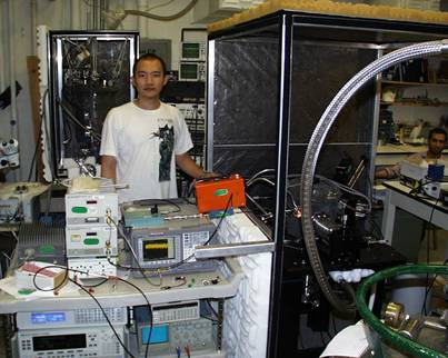
Fig. I1 View of the two cryogenic near-field microwave microscopes at the University of Maryland . Sheng-Chiang Lee (left) and Atif Imtiaz (far right) have since graduated with Physics Ph.D.s. The cryogenic microscope behind Lee is a more conventional STM/microwave microscope (developed by Imtiaz), while the microscope in front and to the right of Lee is the wafer-probe STM/microwave microscope . Lee is now a Professor in the Physics department at Mercer University, and Imtiaz is an NRC post-doc at NIST/Boulder.
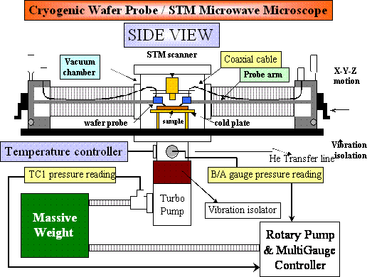
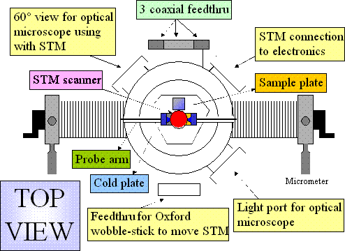
Fig. I2 Schematic view of the cryogenic near field microwave microscope with wafer-probing capabilities built in.
Wave Chaotic Microwave Cavities
We have several microwave cavities for performing quantum chaos experiments. The ¼-bow-tie cavity is shown in Fig. I4. Other quasi-2D cavities include a rectangle, a large circle (originally built for ray-splitting experiments), and a ¼-stadium. We also have several three-dimensional cavities, including a computer box, and a large rectangular enclosure (1.22 meters x 1.22 meters x 0.61 meters) with mode-stirrers inside (see Fig. I5).
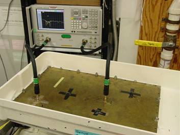
Fig. I4. Bow-tie cavity (flat brass plate) being measured in a 2-port experiment by the Agilent E8364B PNA. The cavity is located in a bath that can be filled with solid CO2 or liquid N2 for cooled cavity experiments. Up to 5 ports can be employed on this cavity.
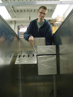
Fig. I5 Interior view of the partially-assembled GigaBox for use with three-dimensional wave chaos studies, along with graduate student Chris Bertrand.
Other Capabilities
A variable magnetic field can be applied to the sample in any of the room temperature microscopes, and two of the cryogenic microscopes. We use an electromagnet to generate variable magnetic fields up to 6 kG in strength. This magnet has been used to image ferromagnetic resonance in manganite materials.
The spatial resolution of our microscopes can also be varied by changing the characteristic size of the inner conductor of the probe, or the size of the parallel strip transmission line. We have demonstrated spatial resolutions between ~2.5 nm up to 1 mm. The larger spatial resolutions are helpful for investigation of gross features of the sample, and can be used to check the homogeneity of film thickness and topography over a substrate, for instance.
Other Resources:
A first class machine shop and electronics shop are available down the hall from the Anlage lab. These important resources have been used to build all of the custom experimental equipment used to carry out our research.
Phone: (301) 405-7321 Fax: (301) 405-3779
Copyright © 2008-2014 University of Maryland
Contact us with comments, questions and feedback