
Anlage Research Group |
| High Frequency Superconductivity, Microscopy, Nanophysics, and Chaos |
Affiliations:
Laser Scanning Microscopy (LSM) is a powerful tool for
non-destructive testing of planar microelectronics chips containing superconducting,
semiconducting and normal-metal elements. The micron-range resolution
of the LSM matches the scale of point and extended defects, and high-temperature
Superconducting (HTS) material grains. These grains are responsible for
the spread of superconducting properties (critical temperature Tc, superconducting
transition width dTc, critical current density
Jc) and for the topology of dc and rf electric transport. Secondly, the
large field of view provided by the LSM (up to tens of millimeters) is
comparable to typical sizes of experimental HTS structures and HTS microchips.
Last, the LSM presently seems to be the only technique which gives the
option of simultaneous imaging and local manipulation of the superconducting
properties of HTSs in a controllable way. We have shown earlier that the
use of the LSM allows confident search and identification of microscopic
defects, individual grain boundaries, spatial irregularities of HTS superconducting
properties, and resistive regions of Ohmic dissipation.
In contrast with common light microscopy, the LSM method utilizes point-by-point raster scanning of the surface of a sample-under-test by employing a sharply focused laser beam as the optical probe. The interaction between the light and the superconductor results in local heating of the superconductor by the absorbed laser power, creating a non-equilibrium perturbation in its electronic system, and change in the intensity and polarization of the reflected beam. These changes are the source of the LSM photoresponse PR(x,y) that is detected as a function of the probe position (x,y) within the sample area. The photoresponse is transformed then into the local LSM contrast voltage V(x,y) to put it into computer for building a 2-D image of the optical, electronic, rf and other properties of the superconductor. The laser power is chosen low enough to consider the perturbation small within the framework of the specific task. The probe intensity is modulated in amplitude with the frequency fM= wM/2p and lock-in detected to enhance the signal-to-noise ratio and hence the contrast. The lock-in detection of the ac component dVAC=0.5 dV(x,y, wM) sin ( wMt + k) at the frequency fM is used (t is time and k is phase shift of the excitation wave).
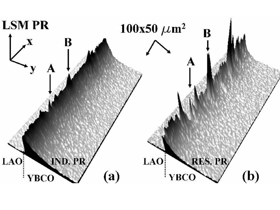
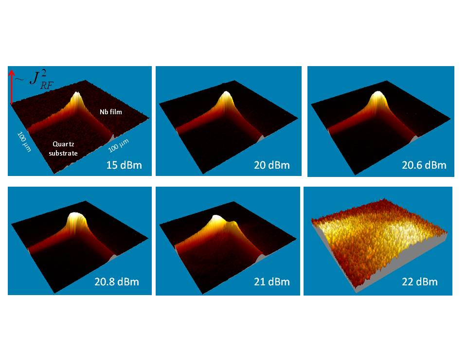
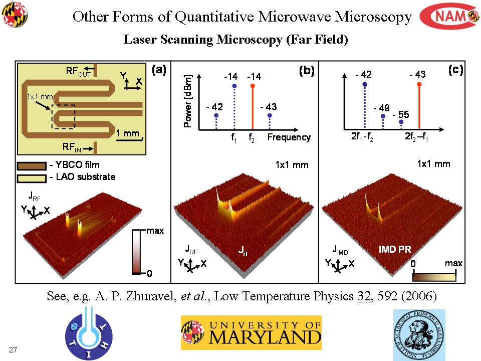
Fig. 1 2D LSM images of (a) inductive and (b) resistive components of LSM PR in the center of a co-planar waveguide HTS microwave device, extracted by using the new procedures described in reference 115, below. The images on the right show the evolution of photoesponse at the inside corner of a superconducting meta-molecule as a function of increasing microwave power. A switching event eventually causes this meta-molecule to change its transmission properties.
Our collaborators in Karlsruhe Germany have a web site describing work done with the scanning laser microscope there.
An NSF-funded project entitled "A Novel Gap Spectroscopy Tool and Discovery of New Nodal Superconductors" is using the LSM to explore new ways to detect nodal directions in the low-energy excitation spectrum of exotic superconductors. This work is based on the methods described in publication 161, below.
This work is done in collaboration with Dr. Alexander Zhuravel of the Verkin Institute of Low Temperature Physics in Kharkov, Ukraine, and Prof. Alexey Ustinov of the Karlsruhe Institute of Technology, Germany. This work is supported by the National Science Foundation under grant number 1410712, the Department of Energy, and the Office of Naval Research.
Unfortunately, our esteemed colleague Alexander Zhuravel has passed away. We deeply miss him and his contagious enthusiasm for superconductivity research. Here is a brief memorial to our colleague Sasha Zhuravel.
Papers: (All papers can be downloaded from the full publication list)
88. A. P. Zhuravel, A. V. Ustinov, K. S. Harshavardhan,
and Steven M. Anlage "Influence of LaAlO3," Surface Topography
on RF Current Distribution in Superconducting Microwave Devices,"
Appl. Phys. Lett. 81, 4979-4981 (2002). pdf
92. A. P. Zhuravel, A. V. Ustinov, D. Abraimov, and Steven M. Anlage, "Imaging Local Sources of Intermodulation in Superconducting Microwave Devices," IEEE Trans. Applied Supercond. 13, 340-343 (2003). pdf
96. A. P. Zhuravel, A. V. Ustinov, K. S. Harshavardhan, S. K. Remillard and Steven M. Anlage, “ Microscopic Imaging of RF Current Distribution and Intermodulation Sources in Superconducting Microwave Devices ,” Mat. Res. Soc. Symp. Proc. Vol. EXS-3, EE9.7.1-EE9.7.3 (2004). pdf
97. Alexander P. Zhuravel, Stephen Remillard , Steven M. Anlage, Alexey V. Ustinov, “ Spatially Resolved Analyses of Microwave and Intermodulation Current Flow Across HTS Resonator Using Low Temperature Laser Scanning Microscopy ,” The Fifth International Kharkov Symposium on the Physics and Engineering of Microwaves, Millimeter, and Submillimeter Waves, Vol. 1, 421 - 423 ( 2004) . cond-mat/0401518. pdf
107. A. P. Zhuravel, Steven M. Anlage, and A. V. Ustinov,
“ Microwave Current Imaging in Passive HTS Components by Low-Temperature
Laser Scanning Microscopy (LTLSM) ,” J. Supercond. 19, 625-632 (2006) . DOI: 10.1007/s10948-006-0123-5 cond-mat/0311511. pdf
111. A. P. Zhuravel, A.G. Sivakov, O.G. Turutanov, A.N. Omelyanchouk, Steven M. Anlage, A.V. Ustinov, "Laser Scanning Microscope for HTS Films and Devices," Low Temperature Physics 32, 592-607 (2006) . cond-mat/0512582. pdf
115. A. P. Zhuravel, Steven M. Anlage, A.V. Ustinov, "Measurement of Local Reactive and Resistive Photoresponse of a Superconducting Microwave Device," Appl. Phys. Lett. 88 , 212503 (2006). cond-mat/0512572. pdf
121. A. P. Zhuravel, Steven M. Anlage, and A. V. Ustinov, Imaging of Microscopic Sources of Resistive and Reactive Nonlinearities in Superconducting Microwave Devices, IEEE Trans. Appl. Supercond. 17 , 902 - 905 (2007).
DOI: 10.1109/TASC.2007.897322 . cond-mat/0609244. pdf
125. Alexander P. Zhuravel, Steven M. Anlage, Stephen Remillard , Alexey V. Ustinov, Spatial Correlation of Linear and Nonlinear Electron Transport in a Superconducting Microwave Resonator: Laser Scanning Microscopy Analysis, The Sixth International Kharkov Symposium on the Physics and Engineering of Microwaves, Millimeter, and Submillimeter Waves. pdf
133. A. P. Zhuravel, Steven M. Anlage, Stephen K. Remillard, A. V. Lukashenko, A. V. Ustinov, “Effect of LaAlO3 Twin-Domain Topology on Local DC and Microwave Properties of Cuprate Films,” J. Appl. Phys. 108, 033920 (2010). pdf
140. Haig A. Atikian, Behnood G. Ghamsari, Steven M. Anlage, and A. Hamed Majedi, “Ultrafast Linear Kinetic Inductive Photoresponse of YBa2Cu3O7-d Meander-Line Structures by Photoimpedance Measurements,” Appl. Phys. Lett. 98, 081117 (2011). pdf
Cihan Kurter, Alexander P. Zhuravel, Alexey V. Ustinov, Steven M. Anlage, “Microscopic examination of hot spots giving rise to nonlinearity in superconducting resonators,” Phys. Rev. B 84, 104515 (2011). pdf
Alexander P. Zhuravel, Cihan Kurter, Alexey V. Ustinov, Steven M. Anlage, “Unconventional RF Photo-Response from a Superconducting Spiral Resonator,” Phys. Rev. B 85, 134535 (2012). pdf
G. Ciovati, Steven M. Anlage, C. Baldwin, G. Cheng, R. Flood, K. Jordan, P. Kneisel, M. Morrone, G. Nemes, L. Turlington, H. Wang, K. Wilson, and S. Zhang, “Low temperature laser scanning microscopy of a superconducting radio-frequency cavity,” Rev. Sci. Instrum. 83, 034704 (2012). pdf
161. A. P. Zhuravel, B. G. Ghamsari, C. Kurter, P. Jung, S. Remillard, J. Abrahams, A. V. Lukashenko, A. V. Ustinov, Steven M. Anlage, “Imaging the Anisotropic Nonlinear Meissner Effect in Nodal YBa2Cu3O7-δ Thin-Film Superconductors,” Phys. Rev. Lett. 110, 087002 (2013). pdf
Gianluigi Ciovati, Steven M. Anlage, and Alexander V. Gurevich, “Imaging of the Surface Resistance of an SRF Cavity by Low-Temperature Laser Scanning Microscopy,” IEEE Trans. Appl. Supercond. 23, 3500506 (2013). pdf
S.K. Remillard, D. Kirkendall, G. Ghigo, R. Gerbaldo, L. Gozzelino, F. Laviano, Z. Yang, N. Mendelsohn, B.G. Ghamsari, B. Friedman, P. Jung, S. M. Anlage, “Microwave Nonlinearity and Photoresponse of Superconducting Resonators with Columnar Defect Micro-Channels,” Supercond. Sci. Technol. 27, 095006 (2014). pdf
Phone: (301) 405-7321 Fax: (301) 405-3779
Copyright © 2008-2025 University of Maryland
Contact us with comments, questions and feedback